Junctions: ChipWizard Professional and Transistors
By gamer_152 0 Comments
Note: The following article contains major spoilers for ChipWizard Professional.
You may have heard that the transistor was one of the most important inventions of the 20th century or one of the most transformative technologies period. And you might wonder why it enjoys that esteemed podium in the history of electronics. In my 20th Century Food Court article, I stressed the significance of logic gates in computers. You'll recall that these circuit elements take some input in, perform a logical operation on it, and then cough up an output. But I left logic gates as black boxes. Electrical signals enter, something happens, and then a different signal exits. So, what's the "something"? How could the same lump of silicon produce different data each time? Well, Zachtronics has a game about that too.
ChipWizard Professional is another exhibit in the studio's Last Call BBS collection, and every puzzle within it commands us to make a computer part out of transistors. Playing the game, we quickly realise the role of these parts: they're switches that either block an electrical charge moving through a circuit or allow that charge through. But where we must manually toggle a physical switch, transistors can open and close their path through the circuit in response to an electrical signal. Because these doors can be controlled electronically, software, rather than a human, can decide where in the device current flows. And software can make many more decisions per second than a person can, making computers the masterminds they are.
The transistors we work with in ChipWizard are "BJTs": Bipolar Junction Transistors. As we see in the play, BJTs come in two types: NPN and PNP. To avoid overloading you, I'm going to start by only describing NPN transistors. Bipolar Junction Transistors connect to the rest of the circuit at three points: the base, the collector, and the emitter. As depicted in the game, if there is no charge coming into the base, no electricity will flow between the collector and emitter. If, however, you route an electrical signal into the base, current will push from the collector to the emitter. You can think of the collector as the entrance, the emitter as the exit, and the base as the lever that opens up the flow.[1]

To have us construct transistors, ChipWizard needs to provide us with the basic materials that can compose them: p-type and n-type silicon. When designing a technology, the materials we choose match what we want that tech to do. When dreaming up our transistor, we know we can't make them out of insulating materials because little charge would flow through them. However, we also can't use anything too greedily conductive because then these parts couldn't dam a circuit. Therefore, engineers make transistors from semiconductors: materials that fall halfway between conductors and insulators on the conductivity spectrum. You've probably heard that silicon is the category killer in this field. What you might not know is that you never use pure silicon for this purpose.[2]
We'll need to go back to high school science to understand why pure semiconductors don't make good transistors. Inside atoms, electrons are arranged into "shells", which we can think of as concentric circles extending outwards from the atom's nucleus.[3]

In reality, electrons aren't little balls that exist at pinpoint locations; they're more like fields, but this illustration of the atom (the Bohr model) reduces friction in our understanding.[3] Electrons are negatively charged, while the protons in the atom's nucleus are positively charged, and those opposites attract, holding the electrons in orbit.[4] The electrons in the shell closest to the nucleus are most strongly attracted to it, while the electrons in the shell furthest from the nucleus (the valence shell) have a higher energy level and drift further from the nucleus than others. Sometimes, the connection between an electron in the valence shell and the nucleus is weak enough that outside forces can knock the electron off the atom.[3]

An electron detached from an atom is a free electron. A free electron can push a loose electron off of another atom, which can displace more electrons, and so on. The potential for outer shell electrons to be knocked free is what we use to define conductors and insulators. Conductors have loosely bound outer electrons that can easily be jailbroken, while insulators refuse to give up their outer electrons. These free electrons moving through the material constitute an electrical current and can also enter the outer shell of other atoms in the material ready to accept them.[4]
Many elements follow the "octet rule", in which they accept or eject electrons until they have eight of them in their valence shell. Atoms can reach eight electrons through importing electrons from or exporting electrons to other atoms. For example, if an atom has nine electrons in its outer shell and it gives one away, it can drop down to eight electrons. But an atom can also become a magic eight ball by forming covalent bonds with other atoms. Covalent bonds are chemical bonds in which atoms attach themselves to each other by sharing electrons. The same electron or electrons will exist in the valence shells of both atoms. It's like two people being stuck in Chinese finger traps and the electrons are the traps.
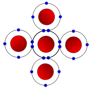
A silicon atom has four electrons in its valence shell.[5] So, if you surround it with four other silicon atoms, and each shares one electron with our central silicon atom, the central atom can reach its goal of eight valence atoms and obey the octet rule. If we surround each of those edge atoms with three more silicon atoms which each donate one electron, it's possible for them to have eight electrons in their outer shell too. Because of the octet rule, silicon will covalently bind together into a neat grid, letting us create the wafers of silicon that we can use in transistors.[6] But we were meant to be making a semiconductor: a material in which electrons could be knocked off of atoms and passed onto other atoms, and that's not going to happen often in this lattice in which every particle has already fulfilled its allotted quota of electrons. These silicon atoms have already reached their target eight electrons and will rarely capture or release those charged particles.
This is one of the great lies of pop science: silicon is not a particularly good semiconductor. Even electrons in this silicon lattice can occasionally be severed from their atoms by outside forces, but their flow is still not free enough for a transistor. But there is some chemistry we can feasibly perform on our element to make it a decent semiconductor.

To reiterate: lone silicon atoms have four electrons in their outer shell, and therefore, can share two electrons with other silicon atoms on four sides. But if you inserted a few atoms with five outer electrons among those silicon atoms, those five-electron atoms would form four covalent bonds with the surrounding silicon. Then, they'd have nine outer electrons, and they'd want to give that extra electron away to drop down to eight outer electrons and close on the octet rule. That freed electron is going to get pushed into the outer shell of a silicon atom in the lattice, which will then try to offload one of its electrons to drop down to eight, which will affect another neighbouring silicon atom, and now, we have an electron being passed through our matrix. Electrons are negatively charged particles, so you have a negative electrical charge propagating through the material.
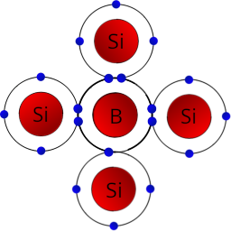
We could, alternatively, seed the silicon with an atom that has three electrons in its outer shell: one down from silicon's four. These three-electron atoms would form covalent bonds with the silicon on three sides, but on the fourth side, they wouldn't have an electron to share with the neighbouring silicon atom. Both the three-electron atom and the fourth adjacent silicon particle will only have seven electrons in their outer shells and will steal an electron from the surrounding lattice to make eight.[6] There is a "hole" (the official term) in the shell that is positively charged, attracting negative particles. Stealing the electron to fill that hole will create a hole in the outer shell of another silicon atom though, which will cause that atom to steal an electron, creating another hole. Now, we have a positive charge bouncing through the wafer.
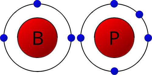
The process of introducing these atoms with five or three outer electrons to the silicon is called "doping". That silicon that has five-electron atoms in it and a negative charge running through it is called n-type silicon. The silicon that has some three-electron atoms and is batting about the positive charges is p-type silicon.[6] N-type "dopants", the ones with five electrons to share, include arsenic, antimony, and phosphorus. P-type dopants, with three valence electrons, include boron, gallium, and aluminium.[7]

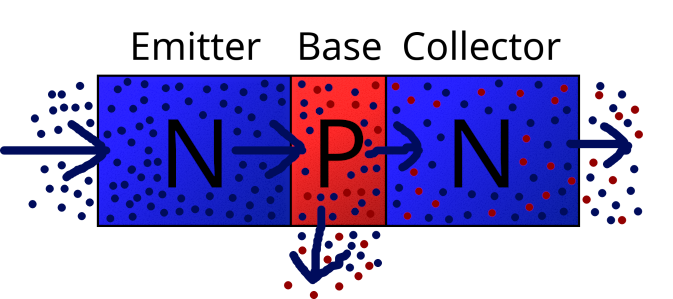
We can observe in ChipWizard that we need both p-type and n-type silicon to make a single bipolar junction transistor. In the game, we fabricate an NPN bipolar junction transistor by drawing a line of blue n-type silicon and then having a line of red p-type silicon overlap it at a 90-degree angle. It's important to understand that in the real transistor, the p-type silicon is not sitting atop the n-type. Instead, you have a bank of p-type silicon with two n-type regions on either side.
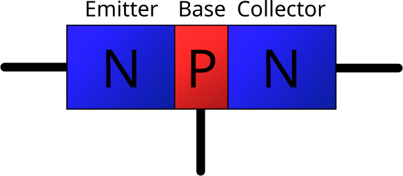
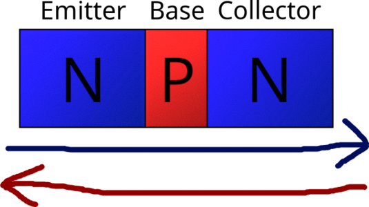
These transistors are "NPN" because if you orient them so the collector is on the left and the emitter is on the right (or vice-versa), reading across, you have some n-type silicon, then p-type, then n-type again. One of those n-type chunks is the collector (the entrance for the electrical current), the smaller p-type stripe in the middle is the base (the gate for the current) and the n-type region on the other side is the emitter (the exit for the current). Remember, n-type has the atoms with excess electrons, and p-type has the atoms with excess holes.
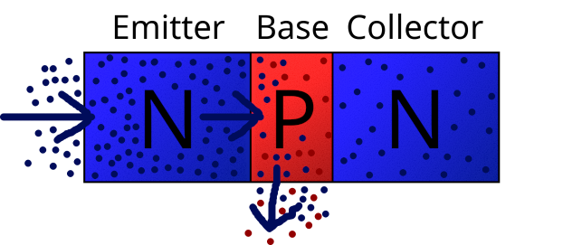
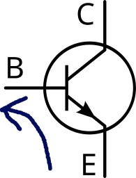
If we push some electrons into the emitter, it will start that long chain of silicon and n-type atoms offloading their electrons. Eventually, the emitter will push its electrons out into the holes in the p-layer that makes up the base. Now, if we have some holes in the atoms outside the base (which we can get by positively charging that portion of the circuit), those electrons will flow out of the base and into the circuit. So, we have a current flowing into the base and out of the emitter. This current is what the arrow on the NPN transistor's circuit symbol indicates.
It might sound like a contradiction that the electrons are flowing from the emitter to the base, but the charge is flowing from the base to the emitter. It takes a minute to wrap your head around, but charges in a circuit proceed in the opposite direction to the electron movement. A charge is not the electrons moving through a circuit; it's the "holes" that those electrons are going to fill propagating. You'll also notice we're not all the way to ungating the circuit. We have electricity moving from base to emitter, but we also want it moving from collector to emitter.
This will happen naturally because the atoms in the p-type base will steal electrons from the n-type collector. This creates a "depletion region" of atoms with holes to fill on the edge of the collector.
The emitter is more liberally doped with n-type atoms than the collector, meaning that the emitter has more electrons to give away, and the collector is more prone to developing holes. With its heaving bag of electrons, the emitter can fill many of the holes in the base. The depletion region in the collector will then grab those electrons from the base. At the same time, a power source can pull electrons away from the side of the collector opposite the base, creating holes for the collector's electrons to fall into. The electrons leaving the collector then create holes deeper into the collector for more of the electrons from the base to fill. Now, we have electrons forcing their way into the emitter, across the base, through the collector, and out of the other side. Or, in terms of conventional current flow, there is a charge entering the collector, moving through the base, and then leaving the emitter. There is a consistent flow of electricity through the entire transistor, and the circuit has been ungated.[1]
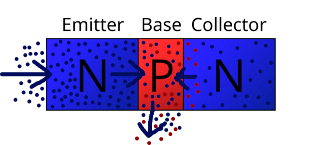
Let's go over the whole journey one more time. The n-type emitter is chock full of five-electron atoms that will form covalent bonds with the surrounding silicon to get nine atoms in their outer shell. This will leave each with an extra atom that it wants to push out to the surrounding silicon to fulfil the octet rule. A chain of electron pushes through the emitter eventually results in electrons gushing into the p-type base. The base is full of three-electron atoms, which will each bond with four silicon atoms to get seven outer electrons. The seven-electron atoms will then steal electrons from the surrounding lattice to achieve their eight valence electrons. The push of electrons from the emitter into the base and the absence of electrons directly outside of the base will then force electrons out of the base into the circuit. We now have quite a strong flow of electrons through the N and P of the NPN transistor, and those particles can force their way into the n-type collector, which will pass the electrons between its atoms until it can push them out into the holes of the circuit on the other side.
Notice that the circuit cannot be completed if there aren't atoms which need electrons outside the base. If the valence shells of the atoms outside the base are full, electrons would just pile up in the centre of the part and have nowhere to go, creating a traffic jam of negative particles. It's in this way that applying the positive charge to the base (making the holes below it) ungates the transistor.


From our comprehension of an NPN BJT, it's easy to learn how the PNP transistor works. The NPN's collector and emitter are n-type, but its base is p-type. For the PNP, it's reversed: the collector and emitter are p-type, and the base is n-type. Inverting the polarity of the parts inverts the current flow through it. Instead of flowing from collector to emitter, the electricity moves from emitter to collector. Instead of applying a positive charge to the base to open up the transistor, you must apply a negative charge, and instead of the charge starting by flowing from base to emitter, it flows from emitter to base.[1]
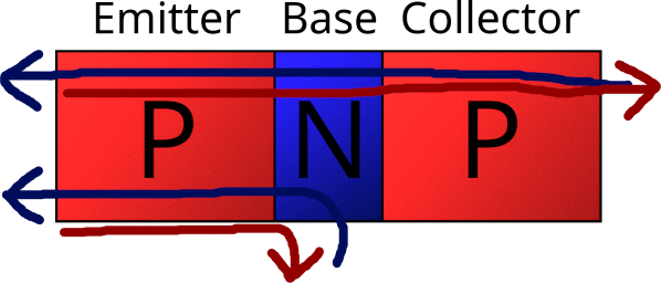
Again, the direction of the charge is displayed on the circuit symbol for the transistor. Compare the NPN icon to the PNP:
![Left: PNP symbol, right: NPN symbol.[8]](https://www.giantbomb.com/a/uploads/original/0/5370/3433528-npnvpnp.png)
ChipWizard, however, uses a fictionalised version of the PNP. Where the game's NPN blocks a charge from flowing through it unless you electrify the base, its PNP allows a charge to flow unless the base receives a signal. That is, the NPN transistor is closed by default, while the PNP is open by default. Not that fiction = bad and non-fiction = good, but if I'm educating on this topic, you should know that that's not how a PNP BJT acts. Definitionally, all transistors only allow a current to flow only once the base is electrified.[2] From a design standpoint, ChipWizard can't model the real difference between an NPN and a PNP transistor because it doesn't implement positive and negative charges or directional current flow. To it, electricity is just electricity and fills up any space it has access to, like water filling pipes. This also means that even ChipWizard's NPN transistors don't have collectors or emitters; a charge will flow from emitter to collector as easily as it flows from collector to emitter.
Now we have a solid understanding of the transistor, we can see how we can implement them in conjunction to form logic gates. Working out how to make logic gates out of transistors is the challenge in the opening stretch of ChipWizard puzzles. Here are a few gates from the game:
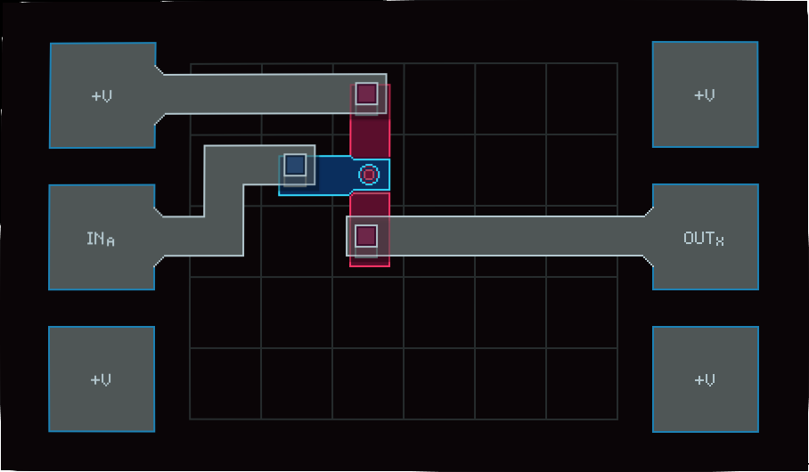
ChipWizard also demonstrates more direct applications for transistors. In one stage, we can connect some transistors' collectors to a power source and its emitters to an alarm. Then, we connect the bases of these transistors to inputs which likely stand in for signals from sensors. When both of the probable sensor signals are "on", or "1", an electrical signal can flow to the alarm.

In a couple of levels, I implemented the AND-OR latch from the previous article: the circuit that lets us store or delete a single bit. In the stage shown below, the bit represents whether a motor is "on" or "off". When the "On" signal is electrified, a charge is sent to the motor until the "off" signal is electrified.
Examples like these show the gargantuan practical potential of the transistor. It's a utility born of its adaptability. Now, I could end the article here and leave you with a litany of misconceptions about electronics, but I don't want to do that. So, let's do some cleanup.
Firstly, we've been discussing how semiconductors work under the free electron theory, but once you get down to a small enough scale, that theory stops making correct predictions. Modern computers pack mucho transistors into very little space to maximise memory capacity and processing power. The modern smartphone transistor is just seven to ten nanometers across, and IBM has been able to fabricate a two-nanometer transistor. For comparison, a typical atom is 0.1 to 0.5 nanometers across. At that zoom level, only quantum mechanics can correctly describe interactions. But, dear god, we can't get any further into quantum physics here.

Secondly, transistors aren't the only non-human-operated switches in circuits. The most famous alternative to the transistor is the vacuum tube which was the standard before the widespread production of transistors. However, the microscopic size, miniscule power consumption, and high speeds of the transistor mean that they beat out opposing technologies.[2]
Thirdly, while we use silicon as our medium in ChipWizard, there are other semiconductors. For example, some transistors are made of germanium, which also has four valence electrons, or the compound gallium arsenide. But silicon has monopolised the business because it's the second most abundant element in the Earth's crust after oxygen, making up more than a quarter of it. Therefore, it's cheap and not going to run out any time soon.
Fourthly, while we're strapping together BJTs in ChipWizard, 99.9% of transistors today are MOSFETs or Metal Oxide Semiconductor Field Effect Transistors. As transistors, MOSFETs are still gates in circuits controlled by an electronic signal, but we use different terminology for their parts, and they have a distinct construction from BJTs. There are many types of MOSFETs, and these aren't the only types of transistors either.
Fifthly, don't get confused into thinking that n-type semiconductors are negatively charged, and p-type semiconductors are positively charged. There are shifting areas of the materials that will carry negative or positive charges when you run a current through them, but when taken as a whole, they all have the same amount of net positive and negative energy, making them electrically neutral.
Sixthly, transistors are not just used to gate sections of circuits; they can also serve as amplifiers or control the amount of power running through part of a circuit.[2] Then there are one or two details that the game is straight-up taking artistic license with. We've discussed that there is no direction of current flow or polarity of charges in the game. We also never have to worry about resistors or electromagnetic interference, or many other challenges a real engineer faces.
Despite its pixelation of electronics, ChipWizard Professional captures the instrumentality of the transistor. Something I appreciate about Zachtronics' library is that it doesn't just consist of detailed descriptions of computer science. The games that comprise it also fit together to form a more comprehensive image of a computer's workings than you could get from any one title. Puzzlers like Exapunks and TIS-100 teach you the rough logic of programming, 20th Century Food Court shows you how that code could be executed by a circuit, and then ChipWizard Professional demonstrates how you might build some of the parts in that circuit. Rather than choosing depth or breadth, Zachtronics games incorporate both, taking you from understanding components in a system to understanding the system as a whole. Thanks for reading.
Notes
- How a transistor works by Ben Eater (Mar 20, 2015), YouTube.
- Definition: Transistor by Rahul Awati (June 2022), TechTarget: What Is?
- 2.5: Arrangement of Electron (Shell Model) by John Hutchinson (Jun 5, 2019), LibreTexts.
- Electricity Explained: The Science of Electricity by US Energy Information Administration Staff (December 17, 2021), US Energy Information Administration.
- Ions of silicon will have more or less than four electrons in their valence shell, but we're talking about non-ionised silicon here.
- How semiconductors work by Ben Eater (Mar 19, 2015), YouTube.
- The Doping of Semiconductors by Carl R. Nave (2017), HyperPhysics.
Image adapted from diagrams by Michel Bakni, licensed under Creative Commons Attribution-ShareAlike 4.0 International.
All other sources linked at relevant points in article.